IT Research Lab
We are skilled at using:
1.Various optical microscopes
2.Ultrasound microscopes
3.SEM system
4.FIB workstation
5.Various etching systems
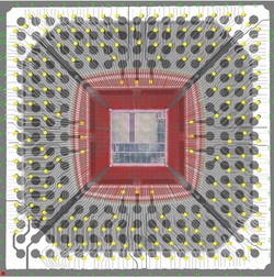
The usual course of IC analysis defined in separate stages: De-capsulation:
We have multiple de-capsulation and de-processing tools and are able process various kinds of packages:
Imaging:
IC de-layering
Accumulated experience in wet etching, plasma-chemical etching and polishing of various kinds of IC samples allows Semiconductors Research to get excellent images of each lithographic layer.
Backside Imaging
With state-of-art etching equipment and accumulated etching methodology we can selectively etch silicon (remains doped area of transistors only) from backside of chip and image the structure of sample.
Scanning electron microscopy (SEM)
This is our key tool for reverse engineering work, where we use a scanning electron beam to provide detailed micrographs with submicron resolution.
Image processing:
Advanced CMOS processes use Multilayer interconnect structures of Aluminum made by Chemical Mechanical Polishing (CMP) or Copper dual Damascene processes. Both structures are dense, dummy filled and content six and more metal layers so is very hard to trace the signal paths and restore interconnection scheme.
Semiconductors Research at first digital processed initial images - extract topology information as wires or vias from each layer separately, second stitch all interconnection layers together with accurate alignment between and next extract the interconnection scheme.
Device analysis:
Semiconductor Research is capable of analyzing all kinds of ICs circuitries, including different process of CMOS, BiCMOS, Bipolar and etc. made by different design rules of Analog, Digital and Mixed-signal.
1.Various optical microscopes
2.Ultrasound microscopes
3.SEM system
4.FIB workstation
5.Various etching systems
The usual course of IC analysis defined in separate stages: De-capsulation:
We have multiple de-capsulation and de-processing tools and are able process various kinds of packages:
Imaging:
IC de-layering
Accumulated experience in wet etching, plasma-chemical etching and polishing of various kinds of IC samples allows Semiconductors Research to get excellent images of each lithographic layer.
Backside Imaging
With state-of-art etching equipment and accumulated etching methodology we can selectively etch silicon (remains doped area of transistors only) from backside of chip and image the structure of sample.
Scanning electron microscopy (SEM)
This is our key tool for reverse engineering work, where we use a scanning electron beam to provide detailed micrographs with submicron resolution.
Image processing:
Advanced CMOS processes use Multilayer interconnect structures of Aluminum made by Chemical Mechanical Polishing (CMP) or Copper dual Damascene processes. Both structures are dense, dummy filled and content six and more metal layers so is very hard to trace the signal paths and restore interconnection scheme.
Semiconductors Research at first digital processed initial images - extract topology information as wires or vias from each layer separately, second stitch all interconnection layers together with accurate alignment between and next extract the interconnection scheme.
Device analysis:
Semiconductor Research is capable of analyzing all kinds of ICs circuitries, including different process of CMOS, BiCMOS, Bipolar and etc. made by different design rules of Analog, Digital and Mixed-signal.
